
Wafer-Level Packaging Trends Reshaping Chip Miniaturization
For decades, chips shrank because transistors shrank. Today, a growing share of the gains in density, speed and power efficiency comes from how dies are packaged together at the wafer level. Fan-out, chip-on-wafer and hybrid bonding are turning packaging from a low-margin back-end step into a strategic front-line technology. Epignosis Insights' review of 2026 data shows capacity, equipment orders and public funding all moving in the same direction.
Why Packaging Now Drives Miniaturization
From single dies to systems in a package
Instead of one large chip, designers now combine multiple smaller dies, or chiplets, with high-bandwidth memory on a shared interposer or wafer. This keeps each die at a manufacturable size while delivering more performance per square millimetre. The complexity is rising fast: more than seven companies can now be involved in a single AI accelerator package, making supply chain design part of product development from day one (Electronics Weekly).
A market growing faster than chips
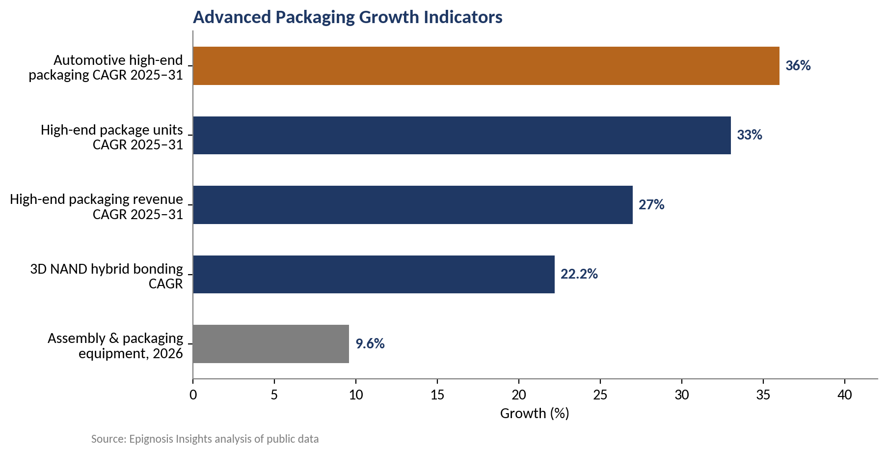
The high-end performance packaging market is forecast to exceed $51 billion by 2031, growing at a 27% compound annual rate from 2025, with package unit volumes rising at 33% a year. The market is highly concentrated, with the six largest players holding about 97% of revenue in 2025, and automotive is the fastest-growing end market at a 36% annual rate (Yole Group).
Chip-on-Wafer Capacity Is the AI Bottleneck
CoWoS scales at record pace
TSMC expects its CoWoS advanced packaging capacity to grow at more than 80% a year between 2022 and 2027 (TSMC). Monthly CoWoS capacity could reach 120,000 to 140,000 wafers in 2026, and with a further 50,000 to 60,000 wafers from outsourced assembly partners, total industry capacity could approach 200,000 wafers per month. Even so, the supply-demand gap is only expected to narrow from around 20% to about 10% by the end of 2026 (TrendForce).
Panel-level packaging is next
As AI packages grow larger than a single reticle, round wafers waste increasing amounts of area at the edges. Moving to rectangular panels allows more large packages per substrate, which is why TSMC and others are developing chip-on-panel approaches. Epignosis Insights expects panel-level production to begin contributing meaningfully from 2028, mainly for the largest AI accelerators.
Hybrid Bonding Pushes Density Further
Orders more than double
Hybrid bonding connects dies copper-to-copper without solder bumps, allowing interconnect pitches below 10 microns and far denser vertical stacking. Equipment maker Besi reported second-quarter 2026 revenue of €249.9 million, up 68.7%, and orders of €292.9 million, up 128.8%, while its hybrid bonding customer base grew from 15 at the end of 2025 to 21 by mid-2026, spanning logic, memory, co-packaged optics and consumer applications (Besi).
Back-end equipment spending rises
Assembly and packaging equipment sales are projected to rise 9.6% to $6.7 billion in 2026, after a 20.8% increase in 2025 (SEMI). Epignosis Insights notes that this figure understates the shift, as much of the investment in chip-on-wafer and hybrid bonding sits in front-end-style tools inside foundry fabs rather than traditional packaging lines.
Beyond the Data Centre
Wafer-level packaging is not only an AI story. Fan-out and fan-in wafer-level packages remain the standard route to thinner smartphones, wearables and hearing devices, where every fraction of a millimetre matters. Automotive is the fastest-growing new frontier, as driver-assistance and central compute modules adopt 2.5D and 3D packaging to fit more processing into tight, heat-constrained spaces. Epignosis Insights expects these segments to adopt technologies first proven in AI accelerators, including hybrid bonding and chiplet designs, with a lag of two to four years as costs fall.
The Challenges Still Ahead
Three issues will shape how fast these trends spread. Yield losses compound as more dies are combined in one package, so a single faulty chiplet can scrap an entire high-value assembly. Heat density rises as dies are stacked, pushing packaging toward liquid cooling and new thermal materials. And costs remain high: advanced packaging steps can now account for a meaningful share of total chip cost, which limits adoption outside premium products. Standards for chiplet interfaces and
testing will be critical to bringing costs down.
Governments Are Funding the Shift
Advanced packaging is now a policy priority. The US National Advanced Packaging Manufacturing Program is offering up to $1.55 billion over five years for packaging research and development, aimed at building a domestic packaging industry capable of handling leading-edge chips (National Institute of Standards and Technology). Epignosis Insights sees similar programmes in Europe, Japan and Korea as a sign that packaging capacity is becoming a strategic asset in its own right.
Epignosis Insights' View
Wafer-level packaging will be the main source of miniaturization gains for AI and high-performance chips through the end of the decade. Capacity will remain tight in 2026 and ease gradually in 2027, but the technology frontier will keep moving toward hybrid bonding, panel-level formats and co-packaged optics.
Companies that control both advanced packaging capacity and hybrid bonding know-how will capture a growing share of chip value, while those relying on conventional packaging risk being left behind.