
The Advanced Packaging Race Behind Silicon Photonics: Why CPO Is Becoming a Manufacturing Challenge
The Integration Economics
Silicon Photonics Is No Longer Just a Photonics Problem
The commercial trajectory of silicon photonics increasingly depends on advanced semiconductor packaging, not just on photonic device design. As optical data rates rise and AI systems demand ever-greater bandwidth density, placing photonic components closer to switching and computing silicon has become increasingly attractive — and increasingly necessary.
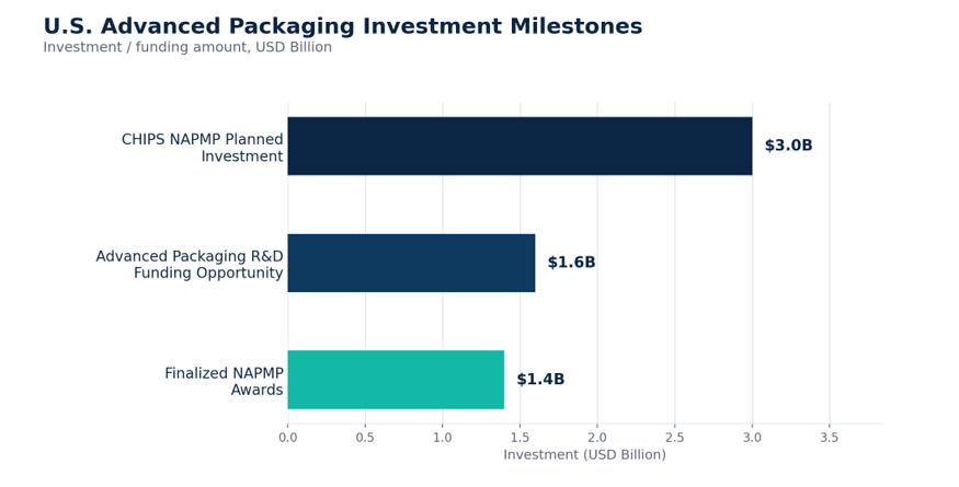
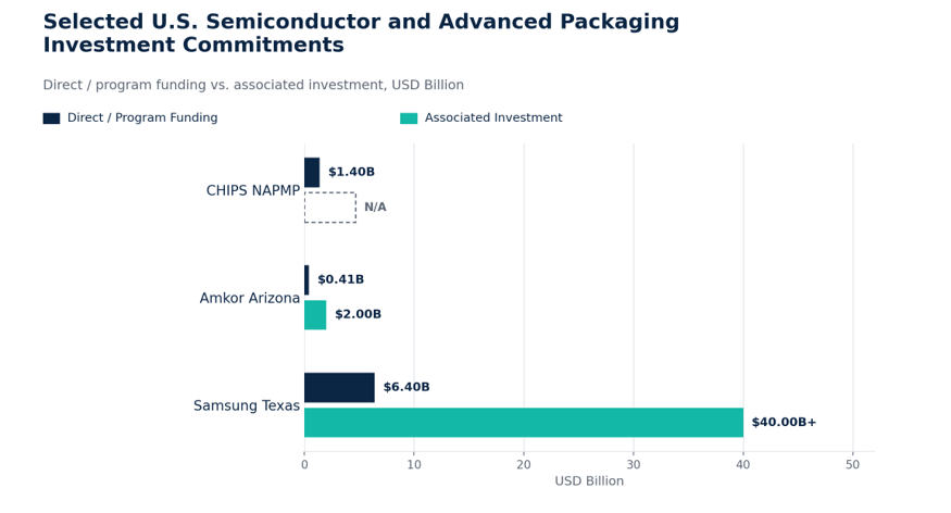
That shift is driving development of co-packaged optics (CPO), optical engines and optical compute interconnects across the industry. In January 2025, the U.S. Department of Commerce announced USD 1.4 billion in finalized awards under the CHIPS National Advanced Packaging Manufacturing Program (NAPMP), part of a broader program built around roughly USD 3 billion in planned investment to develop and scale advanced packaging technologies domestically.
For silicon photonics suppliers, the implication is significant: manufacturing and packaging capability may soon matter as much as photonic design itself.
Why Packaging Is Becoming the Bottleneck
At lower data rates, optical modules can remain relatively separate from the main switching and computing silicon without much penalty. At high data rates, however, the electrical connection between the switching ASIC and the optical engine becomes a genuine limiting factor — signal loss and power draw both climb as that electrical path lengthens.
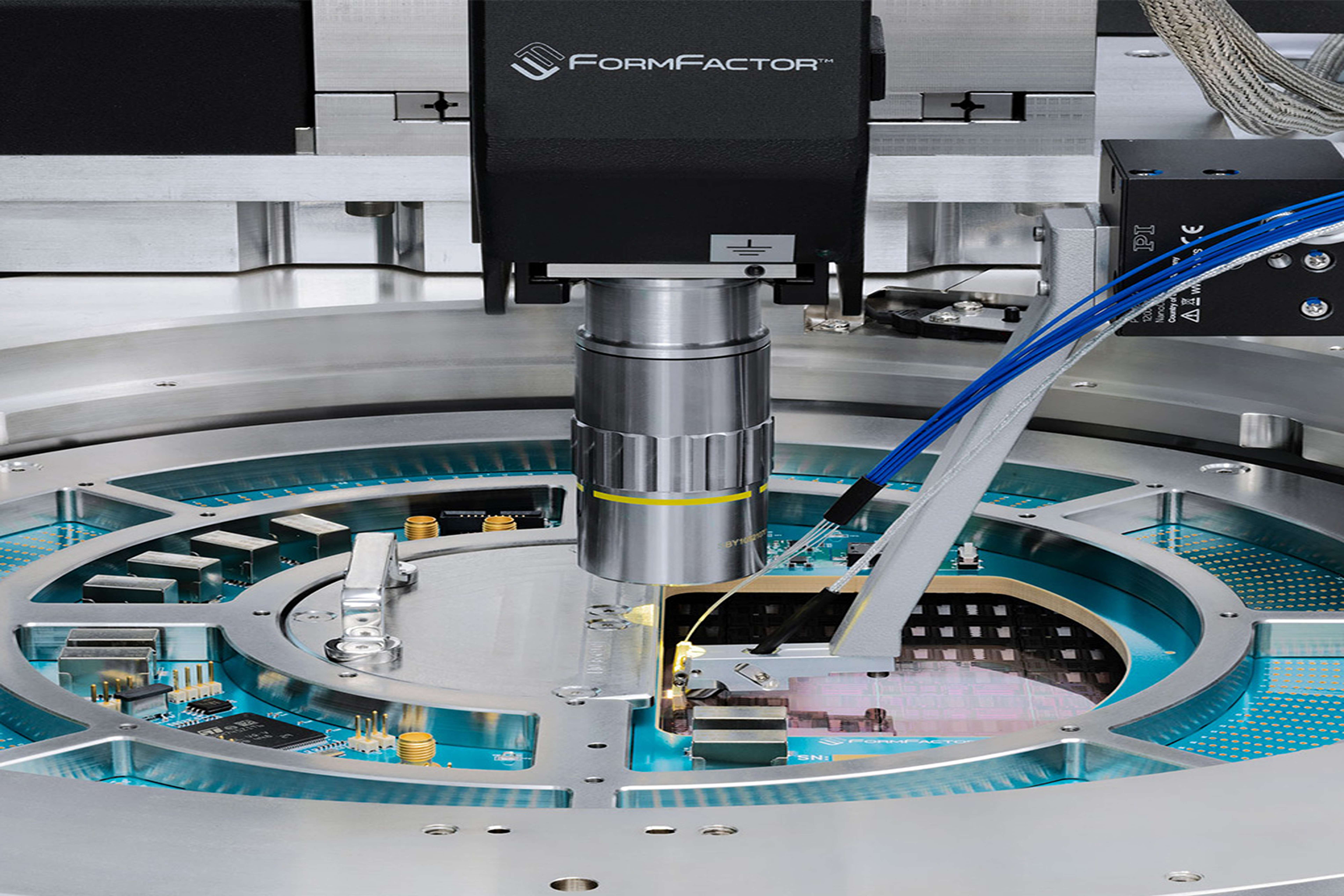
CPO addresses this by moving optical components physically closer to the switching silicon. The concept is technically straightforward to describe but extremely manufacturing-intensive to execute: optical engines, photonic integrated circuits, electrical ICs, substrates, fiber interfaces, and thermal structures all have to operate together as a single, tightly integrated system, not as separately sourced parts bolted together at the end.
Broadcom's CPO Roadmap Shows the Manufacturing Transition
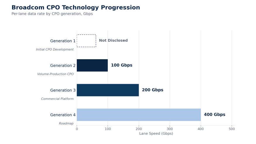
Broadcom's CPO history illustrates the industry's progression from technology demonstration toward genuine volume manufacturing. The company introduced its first-generation CPO platform in 2021. Its second-generation Tomahawk 5-Bailly platform became a volume-production CPO solution, followed by a third-generation platform delivering 200 Gbps per lane that reached commercial availability in 2025. Broadcom has also committed to a fourth-generation, 400 Gbps-per-lane solution. That progression shows CPO development advancing simultaneously on two fronts — optical performance and manufacturing process — rather than one following the other.
From Component to System
Advanced Packaging Is Becoming a Strategic Investment Category
The scale of public investment reinforces just how central packaging has become. The U.S. Department of Commerce announced in July 2024 that CHIPS for America anticipated up to USD 1.6 billion in R&D funding across five advanced-packaging research areas. Six months later, in January 2025, the Department announced the USD 1.4 billion in finalized NAPMP awards referenced above.
These investments extend well beyond silicon photonics, but they are directly relevant to the infrastructure required for advanced optical-electronic integration. The Department of Commerce specifically cites lower power consumption, reduced footprint, higher performance, and chiplet reuse as core benefits of advanced packaging — the same benefits that make CPO and optical compute interconnects attractive for AI infrastructure.
The Supply Chain Is Expanding Beyond Photonics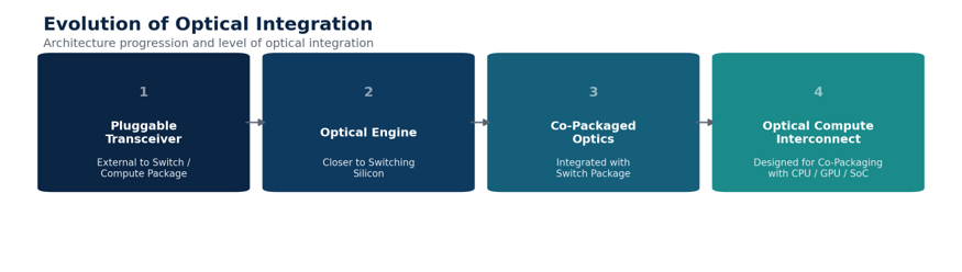
The traditional silicon-photonics supply chain centered on wafers, photonic integrated circuits, lasers, modulators, and optical modules. The emerging supply chain is considerably broader, spanning photonic IC, electrical IC, advanced substrates, optical engines, fiber coupling, thermal interfaces, packages, and the final switch or compute system. That longer chain means companies that control packaging, substrates and assembly can meaningfully influence the economics of the finished optical system — value that used to sit almost entirely with the photonics designer now gets shared across several more players.
Yield Is Becoming a Core Competitive Metric
One of the most important differences between laboratory photonics technology and commercially scalable technology is manufacturing yield. CPO requires several technologies to work correctly simultaneously: semiconductor fabrication, photonic fabrication, optical coupling, packaging, thermal management, and fiber assembly. Broadcom's own description of its third-generation CPO platform explicitly highlights improvements in OSAT (outsourced semiconductor assembly and test) processes, thermal design, handling procedures, fiber routing and yield as central to reaching commercial scale.
Separately, TSMC has reported that its 65-nanometer silicon-photonics process is already in volume production, alongside 3D-stacking technology intended to integrate silicon photonics with high-performance compute for CPO applications; the company has demonstrated 200 Gbps optical signal modulation and greater than 99% 3D-stacking yield on engineering samples. Figures like that illustrate how quickly the packaging ecosystem is catching up to photonic device performance. A technically superior optical architecture that cannot be manufactured consistently at high volume will struggle to compete against a slightly less advanced architecture backed by reliable production economics.
The Manufacturing and Geographic Race
Geographic Competition Is Expanding
The packaging race is also becoming geographic. The United States is investing heavily in domestic advanced packaging capacity through the CHIPS Act. Amkor's Arizona project received up to USD 407 million in direct federal funding and involves roughly USD 2 billion of total investment in a new advanced packaging and test facility.
Samsung's proposed Texas semiconductor ecosystem includes up to USD 6.4 billion in direct CHIPS funding alongside more than USD 40 billion in expected private investment, spanning leading-edge logic, advanced packaging and R&D. These projects are not exclusively silicon-photonics investments. Still, their importance lies in strengthening the broader manufacturing ecosystem on which advanced optical-electronic architectures ultimately depend.
Outlook
The silicon photonics market is likely to move from a component-centric competitive model toward a system-integration model, where the winners are defined as much by manufacturing and packaging capability as by photonic design. Broadcom's transition from 100 Gbps-per-lane volume CPO to a 200 Gbps-per-lane commercial platform and a 400 Gbps-per-lane roadmap demonstrates how quickly that evolution is happening. Intel's 4 Tbps OCI architecture, meanwhile, signals that the longer-term direction extends beyond switch-level CPO toward optical I/O built directly into compute packages.
As a result, advanced packaging should increasingly be treated as a core market driver for silicon photonics in its own right, rather than a supporting manufacturing activity quietly behind the headline photonic technology.
Conclusion
The next phase of silicon photonics will be determined not only by who can design the fastest photonic device, but by who can manufacture and package that device reliably at scale. AI is increasing bandwidth requirements; CPO is moving optics ever closer to switching and compute silicon; and governments and semiconductor companies alike are investing heavily in the advanced packaging infrastructure needed to make it all commercially viable. For investors and technology strategists tracking this market, packaging capability is fast becoming as important a signal as photonic performance itself.