
Silicon Photonics and the AI Power Challenge: Why Optical Connectivity Is Becoming Critical to Data Center Efficiency
Why Power Efficiency Has Become the New Bottleneck for AI Infrastructure
For most of the last two decades, the data center industry measured progress in compute performance: faster chips, denser racks, bigger clusters. That yardstick is no longer sufficient. Silicon photonics is entering a period in which optical connectivity is becoming just as important to AI infrastructure as raw processing power, because AI systems are pushing an unprecedented amount of data between GPUs, CPUs, memory, and networking equipment at the same moment that data centers are confronting a sharp rise in electricity demand.
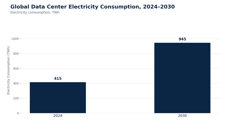
Global data-center electricity consumption reached 415 terawatt-hours in 2024, according to the International Energy Agency. In its base case, the IEA expects that figure to more than double to roughly 945 TWh by 2030. Electricity tied to accelerated servers — the GPU- and AI-heavy machines that power large language models and other AI workloads — is projected to grow around 30% a year, compared with just 9% annual growth for conventional servers. That divergence is reshaping how operators think about every watt in the building.
This changes the role networking plays inside the data center. Optical connectivity is no longer simply a way to move data over long distances between buildings or campuses. It is increasingly becoming a power-efficiency technology in its own right — a lever operators can pull to keep electricity growth from outpacing compute growth.
AI Is Expanding the Data Center Power Requirement
AI workloads create a fundamentally different infrastructure profile than traditional enterprise computing. Large AI clusters depend on high-performance accelerated servers and increasingly dense GPU configurations, which in turn demand far more intensive networking and interconnect capacity than a conventional server farm ever needed.
The IEA expects accelerated servers to account for almost half of the net increase in global data-center electricity consumption through 2030. Conventional servers contribute roughly one-fifth of that growth, while the remainder comes from other IT equipment, cooling and supporting infrastructure.
The resulting pressure is not simply a power-generation problem to be solved by utilities and grid operators. It pushes every component inside the data center to deliver more computing and networking performance per unit of electricity consumed. That is precisely where silicon photonics becomes strategically relevant: it targets the interconnect layer, one of the fastest-growing sources of power draw in an AI cluster.
Optical Connectivity Moves Closer to the Compute
Traditional copper and electrical interconnects are increasingly strained as data rates climb and the physical distances between computing components grow. Electrical traces suffer increasing signal loss at higher speeds and require power-hungry equalization electronics to keep the signal readable.
Silicon photonics tackles the problem differently, using light rather than electrical current to carry high-bandwidth data over the same distances with far less energy loss.
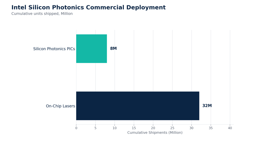
This is no longer a laboratory concept. Intel's commercial silicon-photonics platform has already shipped more than 8 million photonic integrated circuits and more than 32 million on-chip lasers embedded in pluggable optical transceivers for data-center networking, with 400 Gbps, 800 Gbps, and 1.6 Tbps solutions now in its portfolio. That deployment history shows silicon photonics has moved decisively from research into volume commercial infrastructure, and the broader industry is following the same path — moving from stand-alone optical modules toward optical engines and co-packaged architectures where optics sit increasingly close to switching and computing silicon.
The Economics of Faster, More Efficient Optical Links
As AI clusters scale to tens or hundreds of thousands of GPUs, the economic value of every high-speed optical connection rises because network performance directly determines how effectively those expensive compute resources are used. A GPU sitting idle while it waits on data is an extraordinarily costly form of underutilization.
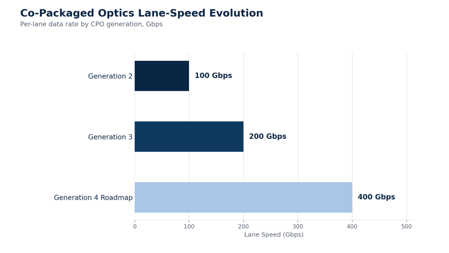
Broadcom's co-packaged optics (CPO) roadmap illustrates where the industry is heading. Its second-generation CPO platform supports 100 Gbps per lane, its third-generation platform doubles that to 200 Gbps per lane, and the company has already committed to a fourth-generation, 400 Gbps-per-lane solution.
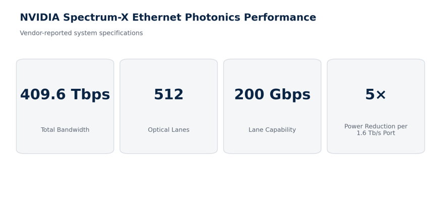
NVIDIA's Spectrum-X Ethernet Photonics architecture shows how this trend translates into AI-scale networking. NVIDIA reports a fivefold reduction in power consumed per 1.6 Tb/s port compared with off-the-shelf Ethernet optics, built around a 512-lane, 200 Gbps-per-lane architecture that delivers 409.6 Tbps of total switch bandwidth. Figures at that scale illustrate why optical connectivity has become a system-level design decision rather than a line-item component purchase.
The Main Constraint Is Integration
Silicon photonics does not eliminate engineering challenges — it shifts a large share of the complexity toward photonic-electronic integration, thermal management, fiber coupling, packaging and manufacturing yield.
Co-packaged optics, in particular, demands tighter integration among optical engines, switching silicon, substrates, connectors, and thermal systems than conventional pluggable transceivers ever required. Broadcom has pointed to improvements in outsourced semiconductor assembly and test (OSAT) processes, thermal design, handling procedures, fiber routing and yield as critical elements of its transition toward 200 Gbps-per-lane CPO. TSMC, meanwhile, has reported that its 65-nanometer silicon-photonics process is already in volume production and has demonstrated 3D-stacking yields above 99% on engineering samples for CPO applications — a sign that the packaging ecosystem is catching up to photonic device performance.
The next competitive battleground for silicon photonics, then, is not simply who can build the fastest photonic device. It is who can manufacture and package that device reliably at high volume.
Outlook
The silicon photonics market is positioned to benefit from two structural trends unfolding simultaneously: rapidly rising AI compute demand and mounting pressure to control data-center electricity consumption. Industry market-engineering estimates put the global silicon photonics market at roughly USD 2.15 billion in 2024, climbing toward USD 3.35 billion by 2026 and reaching an estimated USD 14.19 billion by 2033 — a trajectory implying a compound annual growth rate near 23% for the back half of that period. Shipment volumes of silicon-photonics-enabled transceivers and modules are expected to follow a similar arc, rising from roughly 5.5 million units in 2024 to tens of millions annually by the early 2030s as hyperscalers standardize on optical interconnects for AI clusters.
As data rates move toward 1.6 Tbps and beyond, optical connectivity is moving physically closer to the processor and switch. Competitive advantage will increasingly belong to suppliers that can combine photonic integration, advanced packaging, manufacturing scale and power-efficient optical I/O in a single, reliably manufacturable system.
Conclusion
Silicon photonics is becoming strategically important because the AI infrastructure challenge is no longer only about computing capacity — it is also about moving enormous quantities of data without letting networking power consumption erode the economics of the entire system. The shift from conventional optical transceivers toward optical engines, co-packaged optics and optical compute interconnects therefore represents a genuine architectural transformation, not an incremental upgrade cycle. For data center operators and chip designers alike, power efficiency at the interconnect layer is becoming as decisive a competitive factor as raw compute throughput.