
From 400G to 1.6T: How Silicon Photonics Is Redefining the Data Communication Bottleneck

The Bandwidth Transition
Why Bandwidth, Not Compute, Is Becoming the Next Infrastructure Constraint
The semiconductor industry has spent decades racing to increase processor performance. AI has introduced a different kind of constraint: moving data quickly enough between increasingly powerful computing devices to keep them fed. A GPU cluster is only as fast as the network connecting it, and that network is now being redesigned around optics.
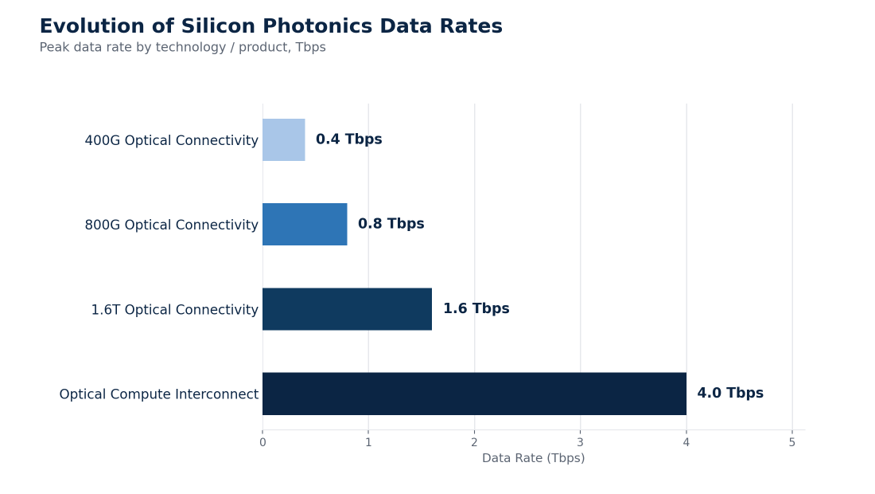
400 Gbps connectivity has become an established high-speed benchmark in data-center networking, while 800 Gbps and 1.6 Tbps solutions are moving into next-generation architectures. Intel's current silicon-photonics portfolio spans 400 Gbps, 800 Gbps and 1.6 Tbps products, and its Optical Compute Interconnect (OCI) chiplet supports 4 Tbps of bidirectional bandwidth — a scale that sits well beyond conventional pluggable transceivers and hints at where the next decade of networking architecture is headed.
This is not an abstract, far-off roadmap. Hyperscale operators are already qualifying 800G optics for production AI clusters today, and early 1.6T deployments are being discussed for next-generation GPU fabrics, which means the timeline for each rung of this bandwidth ladder continues to compress.
The result is a market increasingly defined by bandwidth density rather than simply the number of optical modules shipped. Vendors are competing on how much data a single connection, lane, or chiplet can carry, not just on unit volume.
The Data Rate Ladder Is Moving Up
The march from 400G to 800G and 1.6T is not a routine product refresh. Each generation reflects the growing volume of information that AI training and inference systems must move across the network in real time.
The progression from 400G to 1.6T represents a fourfold increase in per-connection bandwidth in a relatively short span. The 4 Tbps bidirectional capability of Intel's first-generation OCI chiplet points to an even bigger shift: optical connectivity is beginning to move away from traditional pluggable networking and toward direct optical I/O built into compute packages themselves.
The Architecture Shift
Lane Speed Is Becoming the Critical Technology Metric
System bandwidth is determined by more than the headline data rate printed on a transceiver's spec sheet. The underlying lane architecture — how many optical lanes there are and how fast each one runs — determines how efficiently a system can actually scale.

Broadcom's co-packaged optics (CPO) roadmap clearly demonstrates this transition. Its second-generation CPO technology supports 100 Gbps per lane. Its third-generation platform, which reached commercial availability in 2025, moves to 200 Gbps per lane, and Broadcom has already committed to a fourth-generation, 400 Gbps-per-lane solution.
The move from 100G to 200G per lane doubles the bandwidth available from each optical lane without adding physical lanes. A future 400G-per-lane architecture would double it again. That distinction matters because simply adding more physical lanes to hit a bandwidth target increases packaging density, routing complexity and power draw — lane-speed gains avoid much of that cost.
AI Networks Are Moving Toward Hundreds of Terabits
NVIDIA's Spectrum-X Ethernet Photonics platform is built around a 512-lane, 200 Gbps-per-lane architecture that delivers 409.6 Tbps of total switch bandwidth.
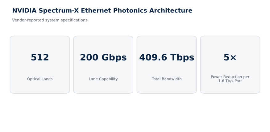
When a single switch reaches hundreds of terabits per second, the electrical and optical interfaces stop being peripheral choices and become central to the overall system design. At that scale, optical connectivity is no longer an accessory bolted onto the switch after the fact — it becomes part of the switch architecture itself, engineered in from the start.
The Integration Challenge
From Pluggable Optics to Optical Compute Interconnect
Traditional pluggable optics keep the optical transceiver physically separate from the switching ASIC, connected by a run of electrical trace. Co-packaged optics moves the optical engine much closer to the switching silicon, shortening the electrical path and reducing the power required to drive it.
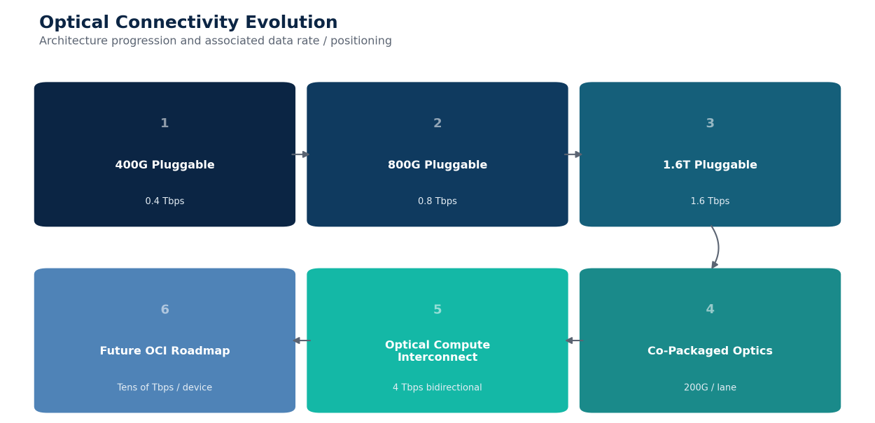
The longer-term development goes further still: optical I/O built directly into compute silicon. Intel's OCI chiplet combines a silicon-photonics photonic integrated circuit — containing on-chip DWDM lasers and semiconductor optical amplifiers — with a CMOS electrical IC in a single package. The first-generation chiplet supports 4 Tbps bidirectional throughput and is designed to be co-packaged with CPUs, GPUs, IPUs, and other system-on-chip devices. The direction of travel is unambiguous: optics keep moving closer to the compute engine, generation after generation.
Bandwidth Growth Creates a Packaging Problem
Higher data rates do not simply demand better photonic devices — they demand better packaging. At higher bandwidth densities, optical engines must be positioned with extremely tight electrical and optical tolerances. Thermal management becomes materially more difficult, fiber routing grows more complex, and manufacturing yield becomes a bigger swing factor in unit economics.
Broadcom has identified thermal design, fiber routing, OSAT (outsourced semiconductor assembly and test) processes, and yield as key areas for development of its third-generation CPO platform. This is a large part of why the silicon photonics market increasingly overlaps with — and depends on — advanced semiconductor packaging, rather than photonics alone.
What Changes Next
Outlook
The transition to 1.6T is a major step forward in optical networking, but the longer-term direction points toward multi-terabit optical I/O built directly into compute packages. Intel's roadmap toward tens of terabits per second per device and Broadcom's commitment to 400 Gbps-per-lane CPO both illustrate how quickly optical interconnect architectures are evolving — with timelines measured in a few years rather than a full decade.
For the broader silicon photonics market, this means growth will increasingly come from higher-value optical integration — CPO, optical engines, OCI chiplets — rather than simply from higher unit volumes of conventional pluggable transceivers. Analysts tracking the space put the global silicon photonics market at roughly USD 2.15 billion in 2024, with a path toward approximately USD 14.19 billion by 2033, a trajectory that assumes exactly this shift toward higher-value, more tightly integrated optical products.
Bottom Line
The central story of silicon photonics is becoming easier to define: AI is increasing the amount of data that must be moved, while next-generation architectures are simultaneously increasing the bandwidth that each optical connection must carry. The transition from 400G to 800G, 1.6T and eventually multi-terabit optical I/O is therefore not merely a speed race between vendors. It is a redesign of the communication architecture at the heart of high-performance computing systems — one that will determine which companies capture the greatest share of value as AI infrastructure continues to scale.