
Yield Rates and Why They Make or Break a New Fab's Profitability
The Math Nobody Puts in the Press Release
A fab groundbreaking announcement always leads with capacity and capital: wafers per month, billions committed, jobs created. What it never leads with is yield, the percentage of chips on a wafer that actually work, because yield is the number that decides whether that capital ever earns a return. The U.S. Government Accountability Office found that CHIPS Act funding recipients had received $30.7 billion in direct awards and $5.5 billion in loans across 40 commercial fab projects by 2025, with Arizona, New York and Texas alone absorbing $26.7 billion of that $36.4 billion. None of that funding guarantees the fabs it builds will yield well enough to be profitable. That has to be earned, node by node, after the ribbon-cutting.
Case in Point: Intel's 18A Ramp
Intel's own investor relations team has been unusually candid about this gap. At Intel's Cisco AI Summit appearance and the RBC Capital Markets technology conference, corporate vice president John Pitzer disclosed that 18A yields have been climbing at roughly 7% per month since mid-2025, a pace he described as consistent with the industry-average trajectory for a new-node ramp. Executives have separately confirmed that Panther Lake wafers produced early in the ramp at Intel's Oregon development fab carry a materially worse cost structure than the higher-yielding wafers coming from Fab 52 in Arizona, a $30 billion facility, as production shifted through 2026. Reporting citing Morgan Stanley in mid-2026 pointed to 18A yields still sitting in roughly the 50% range at wafer sort, well below the levels needed for the node to be broadly profitable across a diverse product mix, even as the monthly improvement trend continued. Chief Financial Officer David Zinsner has been equally direct that Intel does not plan to add significant 18A capacity in 2026, choosing to let yield and demand mature together rather than building ahead of a curve that isn't proven yet.
What a Percentage Point of Yield Is Actually Worth McKinsey's $68 Million Lesson
McKinsey's semiconductor practice quantified this in a case study that remains the clearest public illustration of the stakes: one manufacturer, mapping yield losses across eight major process steps, found it was losing close to $68 million annually to yield-related scrap, with nearly $19 million of that lost at electrical testing alone. A separate manufacturer that set up a dedicated cross-site yield program office delivered a 10% yield improvement and identified $12 million in cost savings within six months of starting the effort. Those are not abstract percentages; they are the direct difference between a fab that clears its cost of capital and one that doesn't, and they explain why semiconductor companies treat yield engineering as a core profit lever rather than a quality-control afterthought.
Why New Nodes Dilute Margins Even at the Best-Run Fabs
Even TSMC, widely regarded as the industry's most consistent yield performer, builds margin dilution from new-node ramps directly into its financial guidance. On its most recent earnings call, the company confirmed that its N2 node entered high-volume manufacturing in the fourth quarter of 2025 with good yield, yet still expects the ramp to dilute corporate gross margin by 2 to 3 percentage points for all of 2026. TSMC separately guided that overseas fab ramps carry a further 2% to 3% dilution in early stages, widening to 3% to 4% in later stages, even once the underlying process is fully qualified. Meanwhile, N3, TSMC's prior-generation node, is only now expected to converge with the corporate average gross margin sometime in 2026, roughly three years after volume production began, a timeline that underscores how long a genuinely well-run yield curve takes to fully pay back its initial ramp costs.
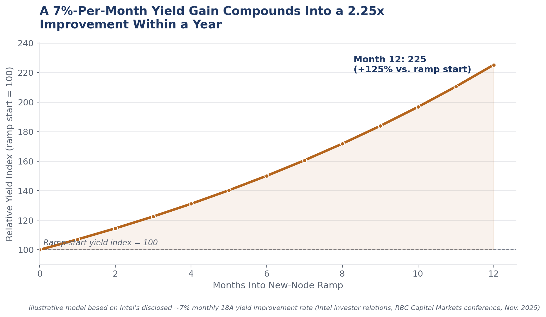
Illustrative compounding model based on Intel's disclosed ~7% monthly 18A yield improvement rate. Source: Intel investor relations, RBC Capital Markets conference, November 2025.
The Capital Stakes Behind Every Yield Curve
These yield curves are being climbed on top of extraordinary fixed costs. SIA and Boston Consulting Group's joint research projects U.S. fab capacity will grow 203% between 2022 and 2032, against a global average increase of just 108%, a buildout the CHIPS Act's $39 billion in manufacturing grants and $13 billion in R&D funding was designed to catalyze, alongside a since-strengthened 35% investment tax credit. SIA's 2025 State of the Industry report ties that expansion to more than 500,000 projected American jobs, including 68,000 direct facility roles, underscoring how much economic activity now sits downstream of a handful of yield curves reaching maturity on schedule. Deloitte's 2026 semiconductor outlook projects the global industry will reach $975 billion in annual sales this year, but also flags that AI chips, while driving roughly half of industry revenue, represent less than 0.2% of total unit volume, meaning the economics of leading-edge yield now sit on a far smaller, far more expensive base of chips than in prior cycles. A fab that ramps slowly on that base doesn't just lose margin points; it risks missing the demand window entirely before yields catch up, handing share to a competitor whose ramp curve simply climbed faster.